HDI technology has emerged as a standard in the design of printed circuit boards due to advancement in the miniaturization of electronic products in the world. Subtypes of PCBs include HDI PCBs which have replaced the previous technologies and standards due to the demand in miniaturization, higher speed, and efficiency of electronic circuits.
In order to satisfy the growing demands of high-speed digital environments, there is a noticeable trend across areas, especially with regard to pcb board in usa markets, towards the implementation of HDI structures in design.
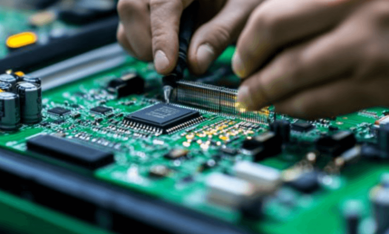
High-Density Interconnect Technology at Its Core
HDI PCBs are more densely packed with connecting pads, and have finer lines and gaps than conventional boards. Microvias, blind and buried vias, and many build-up layers—which enable a higher wiring density per unit area—are some of their distinguishing features. Complex integrated circuits and systems benefit greatly from this high-density arrangement since it can accommodate more input/output (I/O) connections.
The use of computer technology only partly applies to HDI boards since their manfacture reflects highly detailed and complicated processes in terms of design and manufacturing. In contrast with other forms of PCBs, the interlayer connections in HDI are through-hole vias and are not commonly provided by larger droplets but by miniaturized laser-drilled microvias.


New technologies can be successfully integrated into HDI designs without making the final device larger. HDI PCBs are a very alluring choice for companies seeking to provide improved performance without sacrificing form factor.
See also: How Age Better Technology is Transforming Modern Wellness
The Evolution of PCB Design and Manufacturing in America
The PCB board industry in the USA has steadily embraced HDI technology for both prototyping and mass manufacturing as a result of a growing emphasis on innovation and performance. In industries where dependability, form factor, and signal integrity cannot be compromised, these boards are widely used.
The use of HDI PCBs has increased due to the growing need for small, multipurpose devices in the fields of industrial automation, defense, and healthcare. Designers are forced to fit more functionality into smaller spaces as components continue to get smaller while becoming more functional. This demand fits in perfectly with HDI’s capabilities.
A sophisticatedPCB design service plays an even more crucial role in meeting these expectations. Before the first prototype is produced, engineers are modeling, simulating, and optimizing HDI boards using sophisticated software platforms. By accurately analyzing electrical and thermal performance, these design environments can prevent problems in real-world applications.
Given that the USA is still a hub of electronics manufacturing, one has to use the modern-day PCB technologies that can effectively deal with the fast-paced environment. Development teams for PCB boards in the USA now often include HDI design guidelines in their standard procedures, enhancing the nation’s position as a pioneer in cutting-edge electronics.
Superior Design Options Enhancing HDI Performance
Because HDI board structures are inherently complicated, strong and advanced design approaches are required. Microvia placement and signal integrity control via controlled impedance channels are important considerations for routing on HDI PCBs. Routing in crowded spaces, frequently surrounding ICs with a high pin count, is made possible by the use of stacked and staggered microvias.
Power integrity approaches, which guarantee steady voltage transmission between layers without adding undue noise or voltage drops, are also incorporated into advanced design solution strategies. Stabilizing the electrical environment on the board is necessary to enable high-speed digital electronics, and this is accomplished by using distinct power and ground planes.
In HDI designs, thermal control poses a unique set of difficulties. These boards are tiny, thus it’s important to plan heat dissipation channels effectively. Maintaining component dependability requires the use of strategies like thermal vias, embedded heat sinks, and efficient copper balancing.
Managing production tolerances is another benefit of advanced design solution. Even minor variations can lead to performance deterioration or outright failure because HDI boards have smaller geometries and layer counts. The physical structure of the board is guaranteed to closely match the design purpose thanks to close coordination between the fabrication and design teams.
Performance and Dependability in Crucial Applications
In mission-critical systems like medical devices, automotive control units, and aeronautical equipment, reliability is an unavoidable parameter. Because of their multilayer structure and smaller, more consistent features, HDI PCBs provide higher mechanical strength and stability. Better durability across longer life cycles is a result of both the increased density of interconnections and the decrease in through-hole stress.
Additionally, HDI boards’ short connecting routes result in less distortion and delay in the signal, which is essential for high-speed data applications. Because of this performance advantage, HDI PCBs are a crucial part of the design of devices that manage fast data exchange, high bandwidth connectivity, and real-time processing.
Adoption of HDI to Scale Innovation
HDI technology is becoming more and more seen as a doorway to future innovation as devices’ complexity and capabilities continue to advance. Higher bandwidth and reduced latency are required for the ongoing integration of AI, 5G, autonomous systems, and cloud-based solutions, and HDI PCBs are well-positioned to meet these expectations.
Smarter and more efficient devices are emerging as a result of the synergy between HDI PCB capabilities and contemporary electronics requirements. Manufacturers may achieve the kind of optimization that was previously impossible with traditional board designs by using these boards to increase performance without increasing physical dimensions.
By making investments in new design approaches, automation tools, and simulation techniques, PCB design service providers who specialize in HDI technologies are making this transition possible. These services are assisting industries in bringing their ideas to market more quickly and consistently by improving layout accuracy and reducing the development period.
Conclusion
The development of HDI PCBs represents a change in the manufacture of contemporary electronic gadgets. These boards are now crucial for satisfying the requirements of next-generation electronics because they provide a larger interconnect density, better signal integrity, and superior mechanical performance.
HDI is not only a technology of the present; it is a bridge to the future due to the ongoing advancements in PCB boards in US markets and the increasing sophistication of PCB design service providers. By overcoming the difficulties of performance improvement and downsizing, sophisticated design solution techniques have raised the bar for what contemporary PCBs are capable of.
The importance of HDI PCBs will only grow as long as companies keep pushing the envelope of what is conceivable. They are a fundamental component of the architecture of the electronic world of the future because of their ability to spur innovation, reduce form factor, and support high-speed functioning.